7.8 Peeling the crystal
L1 Narrative
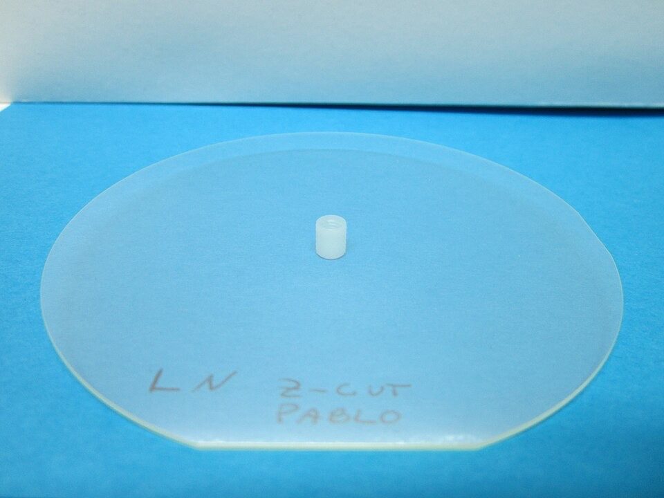
To shrink a lithium niobate waveguide below a micrometer, the crystal itself has to be thin and sit on something with a much lower index. A related method came from silicon. In 1995 Michel Bruel at CEA-LETI in Grenoble implanted hydrogen into silicon, bonded it to another wafer, and heated it until a thin layer split off: Smart Cut [Bruel 1995 rec]. In 1998 a Columbia-led team implanted ions deep into lithium niobate and lifted off 9-micrometer single-crystal films [Levy et al. 1998 rec]. In 2004 ETH Zurich sliced films 680 nm thick onto silicon dioxide and found the electro-optic coefficient intact [Rabiei & Gunter 2004 rec]. Paderborn and Zurich used the name lithium niobate on insulator, LNOI, in a 2012 review, when it already came as 3-inch wafers [Poberaj et al. 2012 rec]. A company in Jinan, NANOLN, founded in 2010, sold the films [NANOLN 2026 rec].
| Damage-layer depth (linear through 3.8 MeV / 10 µm) | 10.0 µm |
| Film, Levy et al. 1998 Levy et al. 1998 | 9 µm |
| Film, Rabiei & Günter 2004 Rabiei & Gunter 2004 | 680 nm |
- Damage-layer depth
- 10.0 µm
- Scale
- sourced pair
- Films reported
- 9 µm (1998), 680 nm (2004)
3.8 MeV and about 10 µm from Levy et al. 1998 (patent, not tied to the paper; other energies on a linear scale through that pair, not a range calculation); films: Levy et al. 1998, Rabiei & Gunter 2004.

L2 Numbers and mechanisms
Ion slicing. Levy et al.: “Deep-ion implantation is used to create a buried sacrificial layer in single-crystal c-cut poled wafers of LiNbO3”; 9 µm films separated and bonded to Si and GaAs [Levy et al. 1998 rec]. The same group's patent gives 3.8 MeV for a damage layer near 10 µm depth and dilute HF etching, without tying them to the paper [Levy et al. 1998 rec]. Rabiei and Gunter: 680 nm films on SiO2 by ion slicing and wafer bonding, crystalline and optical quality comparable to bulk, r33 = 31 pm/V at 633 nm [Rabiei & Gunter 2004 rec]. CEA-LETI transferred LiNbO3 layers by Smart Cut for RF acoustic resonators in 2008-2010 [Pijolat et al. 2008 rec; Moulet et al. 2008 rec; Pijolat et al. 2009 rec; Deguet et al. 2010 rec].
First devices. EO-tunable microrings in a bonded film [Guarino et al. 2007 rec]. Photonic wires by Ar milling down to 1 x 0.73 µm2; 9.9 dB/cm (qTM) and 12.9 dB/cm (qTE) at 1.55 µm [Hu et al. 2009 rec]. LNOI review: sub-micrometer films by ion slicing, two bonding techniques, 3-inch wafers, PP-LNOI SHG, microrings, photonic crystals [Poberaj et al. 2012 rec]. Harvard microdisks: Q about 105, on-chip SHG 0.109 /W [Wang et al. 2014 rec].
Before thin-film wafers. Ridge waveguides were etched into epitaxial Zn-substituted LN by ion-beam enhanced etching: near-vertical sidewalls, 0.9 dB/cm at 1064 nm [Hartung et al. 2008 rec].
Loss, 2009 to 2017 (derived): 9.9 dB/cm [Hu et al. 2009 rec] to 2.7 dB/m = 0.027 dB/cm [Zhang et al. 2017 rec], a factor of about 370.
L3 Sources and status
| Claim | Source | Status |
|---|---|---|
| Smart Cut 1995 (silicon) | Bruel 1995 | rec |
| CIS of LN 1998, 9 µm films | Levy et al. 1998 abstract | rec |
| He ions, 3.8 MeV | Levy et al. 1998 (not tied to paper) | P |
| 680 nm films, r33 31 pm/V | Rabiei & Gunter 2004 abstract | rec |
| “LNOI”, 3-inch wafers by 2012 | Poberaj et al. 2012 abstract | rec |
| NANOLN founded 2010 | company page | rec |
| NANOLN “world-first 3-inch film” 2015 | company claim via news (S); conflicts with Poberaj et al. 2012 | S, disputed (D8) |
References
- Bruel, Electronics Letters 31 1201-1202 (1995). Silicon on insulator material technology. Issued 1995-07-06. doi:10.1049/el:19950805
- Levy et al., Applied Physics Letters 73 2293-2295 (1998). Fabrication of single-crystal lithium niobate films by crystal ion slicing. Issued 1998-10-19. doi:10.1063/1.121801
- Rabiei & Gunter, Applied Physics Letters 85 4603-4605 (2004). Optical and electro-optical properties of submicrometer lithium niobate slab waveguides prepared by crystal ion slicing and wafer bonding. Issued 2004-11-15. doi:10.1063/1.1819527
- Poberaj et al., Laser & Photonics Reviews 6 488-503 (2012). Lithium niobate on insulator (LNOI) for micro‐photonic devices. Issued 2012-02-15. doi:10.1002/lpor.201100035
- About NanoLN (2026). About NanoLN. Issued 2026. www.nanoln.com/ABOUT_NANOLN.html
- M. Levy et al. (1998). US 6540827 B1 (crystal ion slicing of single-crystal films). Issued 1998-02-17. patents.google.com/patent/US6540827B1/en
- M. Pijolat et al., 2008 IEEE Ultrasonics Symposium 201-204 (2008). Large Qxf product for HBAR using Smart Cut ™ transfer of LiNbO3 thin layers onto LiNbO3 substrate. Issued 2008-11. doi:10.1109/ultsym.2008.0049
- J.-S. Moulet et al., 2008 IEEE International Electron Devices Meeting 1-4 (2008). High piezoelectric properties in LiNbO3 transferred layer by the Smart Cut™ technology for ultra wide band BAW filter applications. Issued 2008-12. doi:10.1109/iedm.2008.4796785
- M. Pijolat et al., Applied Physics Letters 95 182106 (2009). Large electromechanical coupling factor film bulk acoustic resonator with X-cut LiNbO3 layer transfer. Issued 2009-11-02. doi:10.1063/1.3258496
- Chrystel Deguet et al., ECS Transactions 33 225-232 (2010). LiNbO3 Single Crystal Layer Transfer Techniques for High Performances RF Filters. Issued 2010-10-01. doi:10.1149/1.3483511
- Andrea Guarino et al., Nature Photonics 1 407-410 (2007). Electro–optically tunable microring resonators in lithium niobate. Issued 2007-07. doi:10.1038/nphoton.2007.93
- H. Hu et al., Optics Express 17 24261 (2009). Lithium niobate photonic wires. Issued 2009-12-21. doi:10.1364/oe.17.024261
- Cheng Wang et al., Optics Express 22 30924 (2014). Integrated high quality factor lithium niobate microdisk resonators. Issued 2014-12-15. doi:10.1364/oe.22.030924
- Holger Hartung et al., Optics Letters 33 2320 (2008). Fabrication of ridge waveguides in zinc-substituted lithium niobate by means of ion-beam enhanced etching. Issued 2008-10-15. doi:10.1364/ol.33.002320
- Zhang et al., Optica 4 1536 (2017). Monolithic ultra-high-Q lithium niobate microring resonator. Issued 2017-12-18. doi:10.1364/optica.4.001536
Events of 7.8
| Date | Event | Who | Ref | St |
|---|---|---|---|---|
| 1995-07-06 | Smart Cut: hydrogen implantation plus bonding for silicon-on-insulator | M. Bruel | DOI | rec |
| 1998-10-19 | Single-crystal LiNbO3 films by crystal ion slicing | M. Levy, R. M. Osgood Jr. +5 | DOI | rec |
| 2004-11-15 | Submicrometer LiNbO3 films by ion slicing and wafer bonding on SiO2, r33 = 31 pm/V | Payam Rabiei, Peter Gunter | DOI | rec |
| 2007-07 | Electro-optically tunable microring resonators in lithium niobate (bonded film) | A. Guarino, G. Poberaj +3 | DOI | rec |
| 2008-10-15 | Ridge waveguides in Zn-substituted LiNbO3 by ion-beam enhanced etching | Holger Hartung, Ernst-Bernhard Kley +3 | DOI | rec |
| 2009-12-21 | Lithium niobate photonic wires from a bonded single-crystal film | H. Hu, R. Ricken +1 | DOI | rec |
| 2010 | NANOLN (Jinan Jingzheng Electronics) established; supplies LNOI and LTOI wafers | URL | rec | |
| 2012-07-16 | 'Lithium niobate on insulator (LNOI) for micro-photonic devices' (review) | G. Poberaj, H. Hu +2 | DOI | rec |
| 2014-12-15 | Integrated high-Q LiNbO3 microdisk resonators | Cheng Wang, Michael J. Burek +2 | DOI | rec |