1801-11-26
Hatchett reports a new metal in a North American mineral and names it columbium
A London chemist finds an unknown metal in an American mineral and calls it columbium.
Charles Hatchett
verified recordDOI
Status of each event: rec verified recordP publication confirmedS secondary onlyderived derived
159 EVENTS V 129 P 7 S 23 D 0
||......|........|.........................|.|...................|..................................................|..........|....................//|........|.|.|.||||||.||||.|||.|.||||.|.|||||||.||||..||..||||||.|..||||||||||
1801                                             1850                                              1900                                               1949                           1980                2000                   2026
| Date | P | Event | Who | Where | Ref | St |
|---|---|---|---|---|---|---|
| 1801-11-26 | D | Hatchett reports a new metal in a North American mineral and names it columbium | Charles Hatchett | Royal Society of London (paper read) | DOI | rec |
| 1802 | Y | Ekeberg names tantalum after Tantalus | Anders Gustaf Ekeberg | Uppsala (attribution) | - | P |
| 1809 | Y | Wollaston argues columbium and tantalum are the same element | William Hyde Wollaston | London | DOI | rec |
| 1818-02-09 | D | Lithium announced: Arfwedson finds a new alkali in petalite; Berzelius names it from Greek lithos | Johan August Arfwedson, Jons Jacob Berzelius | Berzelius laboratory, Stockholm | URL | rec |
| 1844-10-31 | D | Heinrich Rose names niobium after Niobe, daughter of Tantalus | Heinrich Rose | Berlin (Royal Prussian Academy of Sciences, paper read) | DOI | rec |
| 1846-07-16 | D | Rose names a second 'new metal' pelopium after Pelops, Niobe's brother | Heinrich Rose | Berlin (Royal Prussian Academy of Sciences, paper read) | DOI | rec |
| 1866 | Y | Marignac settles niobium chemistry; pelopium and 'ilmenium' are not new elements | Jean Charles Galissard de Marignac | Geneva | URL | rec |
| 1917-04-24 | D | Czochralski publishes the crystal-pulling method (as a way to measure metal crystallization speed) | Jan Czochralski | Berlin (AEG laboratory, attribution) | DOI | rec |
| 1928 | Y | Zachariasen's structure survey of sesquioxides and ABO3 compounds lists LiNbO3 | W. H. Zachariasen | University of Oslo (doctoral thesis) | - | P |
| 1949 | Y | The name niobium chosen internationally over columbium | IUPAC (15th Conference, Amsterdam) | DOI | S | |
| 1949-12-15 | D | Matthias and Remeika find ferroelectricity in LiNbO3 and LiTaO3 | B. T. Matthias, J. P. Remeika | Bell Telephone Laboratories, Murray Hill (byline) | DOI | rec |
| 1958-12 | M | Li2O-Nb2O5 phase diagram | Arnold Reisman, Frederic Holtzberg | IBM (attribution) | DOI | rec |
| 1960-08-01 | D | Bell Labs pulls large CaWO4 crystals by Czochralski for masers | K. Nassau, L. G. Van Uitert | Bell Telephone Laboratories (attribution) | DOI | P |
| 1962-09-15 | D | Theory of light-wave interactions in nonlinear dielectrics, including periodic reversal (quasi-phase matching) | J. A. Armstrong, N. Bloembergen +2 | Harvard University (attribution) | DOI | rec |
| 1964-08-01 | D | Electro-optic properties of LiNbO3 measured | G. E. Peterson, A. A. Ballman +2 | Bell Telephone Laboratories (attribution) | DOI | rec |
| 1964-12-01 | D | LiNbO3: an efficient phase-matchable nonlinear optical material | G. D. Boyd, R. C. Miller +3 | Bell Telephone Laboratories (attribution) | DOI | rec |
| 1965 | Y | Soviet Czochralski growth of LiNbO3, LiTaO3 and NaNbO3 | S. A. Fedulov | USSR (not verified) | - | P |
| 1965-02 | M | Ballman grows LiNbO3 and other piezoelectric and ferroelectric crystals by Czochralski pulling | A. A. Ballman | Bell Telephone Laboratories (attribution) | DOI | P |
| 1965-02-15 | D | Noncritical (90 degree) phase matching in LiNbO3 | R. C. Miller, G. D. Boyd +1 | Bell Telephone Laboratories (attribution) | DOI | rec |
| 1965-06-01 | D | Ferroelectric domain structure of LiNbO3 revealed by etching | K. Nassau, H. J. Levinstein +1 | Bell Telephone Laboratories (attribution) | DOI | rec |
| 1965-06-14 | D | First tunable optical parametric oscillator, in LiNbO3 | J. A. Giordmaine, R. C. Miller | Bell Telephone Laboratories, Murray Hill (OpenAlex affiliation) | DOI | rec |
| 1965-08-01 | D | Elastic wave propagation in lithium niobate | E. G. Spencer, P. V. Lenzo +1 | Bell Telephone Laboratories (attribution) | DOI | rec |
| 1965-12-15 | D | Interdigital transducer: direct piezoelectric coupling to surface elastic waves (on quartz) | R. M. White, F. W. Voltmer | Dept. of Electrical Engineering, UC Berkeley (Crossref affiliation) | DOI | rec |
| 1966 | Y | Electro-optic light modulators (review) | I. P. Kaminow, E. H. Turner | Bell Telephone Laboratories (attribution) | DOI | rec |
| 1966-01 | M | Soviet measurement of the Curie temperature of LiNbO3 | G. A. Smolenskii, N. N. Krainik +3 | USSR (not verified) | DOI | rec |
| 1966-05-01 | D | Electro-optic coefficients of single-domain LiNbO3 | P. V. Lenzo, E. G. Spencer +1 | Bell Telephone Laboratories (attribution) | DOI | rec |
| 1966-06 | M | 'Ferroelectric lithium niobate' parts 1-5: growth, single-domain poling, X-ray and neutron structure | K. Nassau, H. J. Levinstein +5 | Bell Telephone Laboratories (Hamilton: Brookhaven) (attribution) | DOI | rec |
| 1966-07-01 | D | Optically induced refractive-index inhomogeneities ('optical damage') discovered in LiNbO3 and LiTaO3 | A. Ashkin, G. D. Boyd +5 | Bell Telephone Laboratories, Murray Hill (byline) | DOI | rec |
| 1967 | Y | Crystal Technology (Palo Alto) begins making oxide single crystals including LiNbO3 | Crystal Technology, Inc., Palo Alto | URL | rec | |
| 1967-07-01 | D | Field annealing reduces damage susceptibility | H. J. Levinstein, A. A. Ballman +3 | Bell Telephone Laboratories (attribution) | DOI | rec |
| 1968-01 | M | Commercial LiNbO3 crystals are lithium-deficient | P. Lerner, C. Legras +1 | France (attribution) | DOI | rec |
| 1968-10-01 | D | Holographic storage in lithium niobate | F. S. Chen, J. T. LaMacchia +1 | Bell Telephone Laboratories, Murray Hill (byline) | DOI | rec |
| 1969-07-01 | D | Charge-drift model of optically induced index change | F. S. Chen | Bell Telephone Laboratories (attribution) | DOI | rec |
| 1971-04-01 | D | Congruent melting composition located at 48.6 mol% Li2O | J. R. Carruthers, G. E. Peterson +2 | Bell Telephone Laboratories (attribution) | DOI | rec |
| 1971-06-15 | D | Thermal fixing of holograms in electro-optic crystals | J. J. Amodei, D. L. Staebler | RCA Laboratories, Princeton (attribution) | DOI | rec |
| 1971-09-01 | D | Iron impurities identified as the origin of optical damage | G. E. Peterson, A. M. Glass +1 | Bell Telephone Laboratories (attribution) | DOI | rec |
| 1972-02-01 | D | Transition-metal doping and fixing techniques for holographic recording in LiNbO3 | J. J. Amodei, W. Phillips +1 | RCA Laboratories, Princeton (OpenAlex affiliation) | DOI | rec |
| 1972-03-01 | D | Large-coupling leaky surface waves on 64 degree rotated Y-cut LiNbO3 | Kazuhiko Yamanouchi, Kimio Shibayama | Research Institute of Electrical Communication, Tohoku University, Sendai (Crossref affiliation) | DOI | rec |
| 1973-05-15 | D | 'Thin-film LiNbO3 electro-optic light modulator': an out-diffused planar guide in bulk LN, 3.2 GHz | I. P. Kaminow, J. R. Carruthers +2 | Bell Telephone Laboratories, Crawford Hill/Holmdel and Murray Hill (byline) | DOI | rec |
| 1974-01 | M | Earliest paper title found using 'photorefractive' | H. Kurz | Philips Research, Hamburg (attribution) | DOI | P |
| 1974-08-15 | D | High-voltage bulk photovoltaic effect identified as the photorefractive driver in LiNbO3 | A. M. Glass, D. von der Linde +1 | Bell Telephone Laboratories (attribution) | DOI | rec |
| 1974-10-01 | D | Diffusion kinetics of Li2O out-diffused waveguides in LiNbO3 and LiTaO3 | J. R. Carruthers, I. P. Kaminow +1 | Bell Laboratories (OpenAlex affiliation) | DOI | rec |
| 1974-10-15 | D | Metal (Ti) in-diffused optical waveguides in LiNbO3 | R. V. Schmidt, I. P. Kaminow | Bell Telephone Laboratories (attribution) | DOI | rec |
| 1974-11-15 | D | Beam scanning in epitaxial LiNbO3 film waveguides | P. K. Tien, S. Riva-Sanseverino +1 | Bell Telephone Laboratories (attribution) | DOI | rec |
| 1976 | Y | Optimum 127.86 degree rotated Y-cut, X-propagating LiNbO3 for SAW filters | K. Shibayama, K. Yamanouchi +2 | Tohoku University (attribution; affiliation not on the Crossref record) | DOI | rec |
| 1977-08 | M | Fridkin's mechanism for the bulk photovoltaic effect and optical damage | V. M. Fridkin | Institute of Crystallography, USSR Academy of Sciences, Moscow (attribution; byline seen on his 1984 review) | DOI | rec |
| 1977-12 | M | Transient energy transfer during hologram formation in LiNbO3 in an external field | N. Kukhtarev, V. Markov +1 | Kyiv (attribution, not byline-checked) | DOI | rec |
| 1978-01 | M | Band-transport model of photorefractive recording ('Kukhtarev equations') | N. V. Kukhtarev, V. B. Markov +3 | Institute of Physics, Kyiv (attribution, not byline-checked) | DOI | rec |
| 1980 | Y | SAW filters reach practical use in television receivers (Japan) | Michio Kadota (retrospective author) | Murata Manufacturing (author affiliation) | URL | S |
| 1980-03-31 | D | Theory review: the photogalvanic (bulk photovoltaic) effect in media lacking a center of symmetry | V. I. Belinicher, B. I. Sturman | USSR (not verified) | DOI | rec |
| 1980-06 | M | MgO doping raises the optical-damage resistance of LiNbO3 (conference abstract) | Zhong Ji-guo, Jin J. +1 | DOI | P | |
| 1980-10-01 | D | SHG enhanced in LiNbO3 crystals grown with periodic laminar ferroelectric domains (first QPM experiment in LN, standard attribution) | Duan Feng, Nai-Ben Ming +5 | Institute of Solid State Physics, Nanking University (Crossref byline) | DOI | rec |
| 1982-08 | M | Waveguide electro-optic modulators (review) | R. C. Alferness | Bell Laboratories (attribution) | DOI | rec |
| 1982-10-01 | D | Proton exchange in benzoic acid for high-index LiNbO3 waveguides | J. L. Jackel, C. E. Rice +1 | Bell Laboratories (attribution) | DOI | rec |
| 1983 | Y | Heavily Mg-doped LiNbO3: growth and 2 W average second-harmonic power | Zhong Ji-guo, Xu Guan-feng +2 | Southwest Institute of Technical Physics, Chengdu (journal metadata) | DOI | rec |
| 1984 | Y | Shin-Etsu Chemical develops lithium tantalate crystals | Shin-Etsu Chemical Co., Ltd. | URL | rec | |
| 1984-05-01 | D | Increased optical damage resistance in MgO-doped lithium niobate | D. A. Bryan, R. Gerson +1 | McDonnell Douglas Astronautics (Bryan), University of Missouri-Rolla (Gerson), Greenville College (Tomaschke) (byline per) | DOI | rec |
| 1985 | Y | RF SAW filters on 40-70 degree rotated YX-cut LN and LT become practical | Japanese SAW industry | URL | S | |
| 1985 | Y | First commercially available guided-wave modulator (high-speed intensity modulator) | Crystal Technology, Inc., Palo Alto | DOI | rec | |
| 1985-08 | M | "Lithium niobate: summary of physical properties and crystal structure" | R. S. Weis, T. K. Gaylord | Georgia Tech | DOI | rec |
| 1987-11 | M | Stoichiometric LiNbO3 single-crystal fibers by vapor transport equilibration | Y. S. Luh, M. M. Fejer +2 | Stanford University (attribution) | DOI | rec |
| 1989-02-02 | D | Green SHG in a periodically poled planar LiNbO3 waveguide | E. J. Lim, M. M. Fejer +1 | Stanford University (attribution) | DOI | rec |
| 1989-03-13 | D | Photorefraction in Ti:LiNbO3 waveguides studied at Sumitomo Metal Mining | T. Fujiwara, S. Sato +1 | Electronics Materials Laboratory, Sumitomo Metal Mining, Ome (Crossref affiliation) | DOI | rec |
| 1989-05-25 | D | Blue SHG in a periodically poled LiNbO3 channel waveguide | E. J. Lim, M. M. Fejer +2 | Stanford University; IBM (Kozlovsky) (attribution) | DOI | rec |
| 1989-10-26 | D | Laser oscillation in a single-mode Nd:MgO:LiNbO3 channel waveguide | E. Lallier, J. P. Pocholle +7 | France (affiliations not byline-checked) | DOI | rec |
| 1990 | Y | Annealed erbium-implanted single-mode LiNbO3 waveguides (postdeadline) | R. Brinkmann, Ch. Buchal +3 | Universitat Paderborn (attribution) | DOI | rec |
| 1990-01-08 | D | Blue QPM SHG in LiNbO3 with periodic domains grown by laser-heated pedestal growth | G. A. Magel, M. M. Fejer +1 | Stanford University (attribution) | DOI | rec |
| 1990-09-15 | D | Zinc as an optical-damage-resistant dopant in LiNbO3 | T. R. Volk, V. I. Pryalkin +1 | Institute of Crystallography, USSR Academy of Sciences (Volk); Moscow State University (Pryalkin, Rubinina) (Optica byline) | DOI | rec |
| 1991-02-28 | D | Er-doped Ti:LiNbO3 waveguide laser at 1.532 µm ('first integrated optical laser in LiNbO3' per the authors) | R. Brinkmann, W. Sohler +1 | Universitat Paderborn (Crossref affiliation) | DOI | rec |
| 1992 | Y | QPM second-harmonic generation: tuning and tolerances | M. M. Fejer, G. A. Magel +2 | Stanford University (attribution) | DOI | rec |
| 1992-02 | M | Stoichiometric LiNbO3 grown by double-crucible Czochralski with automatic powder supply | K. Kitamura, J. K. Yamamoto +3 | NIRIM, Tsukuba (attribution; affiliation seen on Kitamura's 2000 APL, not on this paper) | DOI | rec |
| 1992-02 | M | Low DC-drift Ti:LiNbO3 modulator assured over 15 years | M. Seino, T. Nakazawa +4 | Fujitsu Laboratories; Fujitsu Ltd (Optica byline) | DOI | rec |
| 1993-02-01 | D | Electric-field periodic poling of LiNbO3 at room temperature for first-order QPM blue SHG | M. Yamada, N. Nada +2 | Corporate Research Laboratories, Sony Corporation, Tokyo (Crossref byline) | DOI | rec |
| 1993-05-01 | D | DC drift of Ti:LiNbO3 modulators studied at Sumitomo Cement | Hirotoshi Nagata, Kazumasa Kiuchi | Central Research Laboratories, Sumitomo Cement, Funabashi (Crossref affiliation) | DOI | rec |
| 1993-06-01 | D | 5000 holograms angle-multiplexed in one Fe:LiNbO3 crystal | F. H. Mok | Electronics Systems Division, Northrop Corporation, Hawthorne CA (byline) | DOI | rec |
| 1994-09-01 | D | Optical-damage-resistant impurities in lithium niobate (review) | T. Volk, N. Rubinina +1 | Moscow; Osnabruck (attribution) | DOI | rec |
| 1994-10-01 | D | Sumitomo Cement and Osaka Cement merge into Sumitomo Osaka Cement | Sumitomo Osaka Cement | URL | rec | |
| 1995-01-01 | D | Quasi-phase-matched 1.064 µm pumped OPO in bulk periodically poled LiNbO3 | L. E. Myers, W. R. Bosenberg +4 | Stanford Ginzton Laboratory; Lightwave Electronics (OpenAlex affiliation) | DOI | rec |
| 1995-07-01 | D | Uniphase buys United Technologies Photonics (LN integrated optics, Bloomfield CT) | Uniphase; United Technologies Photonics | URL | S | |
| 1995-07-01 | D | UTP engineers: external modulation first deployed in telecom on submarine routes | F. J. Leonberger, S. W. Merritt +1 | Uniphase Telecommunications Products (vendor authors) | URL | S |
| 1995-07-06 | D | Smart Cut: hydrogen implantation plus bonding for silicon-on-insulator | M. Bruel | LETI-CEA, Grenoble (byline per) | DOI | rec |
| 1995-11-01 | D | Quasi-phase-matched OPOs in bulk PPLN (full paper) | L. E. Myers, R. C. Eckardt +4 | Stanford University; Lightwave Electronics; Cygnus Laser (OpenAlex affiliation) | DOI | rec |
| 1997 | Y | EOSPACE formed in Redmond WA as a spin-out of Boeing integrated optics | Suwat Thaniyavarn | EOSPACE, Inc. | URL | rec |
| 1997-02-01 | D | OC-192 (10 Gb/s) lithium niobate modulators described by UTP engineers | J. Lin, P. Sanders | Uniphase Telecommunications Products (vendor authors) | URL | S |
| 1997-10-15 | D | Temperature-dependent Sellmeier equation for n_e of congruent LiNbO3 | Dieter H. Jundt | Crystal Technology (attribution, not verified) | DOI | rec |
| 1997-10-31 | D | Quasi-phase-matched third-harmonic generation in a quasi-periodic optical superlattice (LiTaO3) | Shi-ning Zhu, Yong-yuan Zhu +1 | National Laboratory of Solid State Microstructures, Nanjing University (Crossref) | DOI | rec |
| 1998-05-01 | D | Lucent X2600 LN modulator family for 10 and 20 Gb/s | Lucent Technologies Microelectronics Group | URL | S | |
| 1998-10-19 | D | Single-crystal LiNbO3 films by crystal ion slicing | M. Levy, R. M. Osgood Jr. +5 | Columbia; Penn State; Lehigh; SUNY Albany (Crossref) | DOI | rec |
| 1999-06-28 | D | JDS Fitel and Uniphase merge into JDS Uniphase; Ramar (LN integrated optics) acquired 1999-10 | JDS Uniphase | URL | S | |
| 2000-01 | M | Review of lithium niobate modulators for fiber-optic communications | E. L. Wooten, K. M. Kissa +9 | JDS Uniphase, Bloomfield CT (OpenAlex affiliation, all authors) | DOI | rec |
| 2000-09 | M | Photline Technologies founded in Besancon from FEMTO-ST | Henri Porte | Photline Technologies | - | S |
| 2000-09-27 | D | Corning agrees to buy Pirelli's optical components unit (Milan), including LN modulators, for about $3.6 B | Corning; Pirelli; Cisco (10%) | URL | S | |
| 2000-10 | M | Oxide Corporation founded (Yamanashi) to commercialize 'Super LN/LT' crystals | Yasunori Furukawa | Oxide Corporation | URL | rec |
| 2003 | Y | SiO2/Cu/YX-LN Love-wave duplexer reaches practical use | Murata Manufacturing | URL | S | |
| 2003-03-05 | D | Codeon (Mach-10 and Mach-40 LN modulators) merges with Quantum Photonics to form Covega | Codeon; Covega | URL | S | |
| 2003-04-03 | D | Direct-bonded QPM-LN ridge waveguide with high damage resistance at room temperature | Y. Nishida, H. Miyazawa +3 | NTT Photonics Laboratories, Atsugi (Crossref affiliation) | DOI | rec |
| 2004-11-15 | D | Submicrometer LiNbO3 films by ion slicing and wafer bonding on SiO2, r33 = 31 pm/V | Payam Rabiei, Peter Gunter | ETH Zurich (Crossref affiliation) | DOI | rec |
| 2007-07 | M | Electro-optically tunable microring resonators in lithium niobate (bonded film) | A. Guarino, G. Poberaj +3 | ETH Zurich (OpenAlex affiliation) | DOI | rec |
| 2008-10-15 | D | Ridge waveguides in Zn-substituted LiNbO3 by ion-beam enhanced etching | Holger Hartung, Ernst-Bernhard Kley +3 | Jena (attribution) | DOI | rec |
| 2009-09-14 | D | Fujitsu introduces a DP-QPSK LN modulator for 100 Gb/s networks | Fujitsu Optical Components | URL | rec | |
| 2009-09-17 | D | MgO:PPLN chips for 1060 to 530 nm green in pico-projectors | Crystal Technology (EPCOS subsidiary) | - | S | |
| 2009-12-21 | D | Lithium niobate photonic wires from a bonded single-crystal film | H. Hu, R. Ricken +1 | Universitat Paderborn (attribution) | DOI | rec |
| 2010 | Y | NANOLN (Jinan Jingzheng Electronics) established; supplies LNOI and LTOI wafers | Jinan Jingzheng Electronics Co., Ltd. (NANOLN), Jinan | URL | rec | |
| 2011-04-01 | D | Gooch & Housego acquires Crystal Technology, LLC (Palo Alto LN and TeO2 growth) | Gooch & Housego | URL | rec | |
| 2011-11 | M | Sumitomo Osaka Cement sets up an optical-communication parts subsidiary in Guangdong | Sumitomo Osaka Cement | URL | rec | |
| 2012-07-16 | D | 'Lithium niobate on insulator (LNOI) for micro-photonic devices' (review) | G. Poberaj, H. Hu +2 | ETH Zurich; Universitat Paderborn (attribution) | DOI | rec |
| 2014-12-15 | D | Integrated high-Q LiNbO3 microdisk resonators | Cheng Wang, Michael J. Burek +2 | Harvard University (attribution) | DOI | rec |
| 2017-02-15 | D | Heterogeneous LN/SiN waveguides for wafer-scale PICs on silicon | Lin Chang, Martin H. P. Pfeiffer +4 | UCSB; EPFL (attribution) | DOI | rec |
| 2017-12-20 | D | Monolithic ultra-high-Q LiNbO3 microring resonator: Q = 1e7, 2.7 dB/m | Mian Zhang, Cheng Wang +3 | Harvard University (attribution) | DOI | rec |
| 2018 | Y | HyperLight founded as a Harvard spin-out (Cambridge MA) | Mian Zhang (CEO), Christian Reimer (co-founder) | HyperLight Corporation | - | S |
| 2018-01-22 | D | Nanophotonic LiNbO3 electro-optic modulators, 1.8 V cm | Cheng Wang, Mian Zhang +3 | Harvard; Columbia (attribution) | DOI | rec |
| 2018-09-03 | D | Bonded thin-film LN on foundry silicon photonics, > 106 GHz 3 dB electrical bandwidth | Peter O. Weigel, Jie Zhao +3 | UC San Diego; Sandia (attribution) | DOI | rec |
| 2018-10 | M | Integrated LN electro-optic modulators at CMOS-compatible voltages | Cheng Wang, Mian Zhang +6 | Harvard; Nokia Bell Labs (attribution) | DOI | rec |
| 2018-10-02 | D | Arthur Ashkin, first author of the 1966 optical-damage paper, shares the Nobel Prize in Physics for optical tweezers | Arthur Ashkin | Bell Laboratories (Nobel record affiliation) | URL | rec |
| 2018-11-20 | D | Nanophotonic PPLN waveguides: 2600%/W cm^2 SHG at 1.5 µm, 4 µm poling period | Cheng Wang, Carsten Langrock +6 | Harvard; Stanford (attribution) | DOI | rec |
| 2019-02-28 | D | Monolithic LN circuits for Kerr comb generation, filtering and modulation | Cheng Wang, Mian Zhang +4 | Harvard (attribution) | DOI | rec |
| 2019-03-20 | D | Ultra-low-loss visible TFLN photonics | B. Desiatov, A. Shams-Ansari +3 | Harvard | DOI | rec |
| 2019-04 | M | Broadband electro-optic frequency comb in an LN microring | Mian Zhang, Brandon Buscaino +2 | Harvard (attribution) | DOI | rec |
| 2019-05 | M | Hybrid silicon and LN Mach-Zehnder modulators for 100 Gbit/s and beyond | Mingbo He, Mengyue Xu +3 | Sun Yat-sen University (attribution) | DOI | rec |
| 2019-11-28 | D | Lumentum sells its LN modulator product lines (San Donato, Italy) to Advanced Fiber Resources | Lumentum; Advanced Fiber Resources (Zhuhai) | URL | S | |
| 2019-12-20 | D | Periodically poled thin-film LN microrings, SHG efficiency 250,000%/W | Juanjuan Lu, Joshua B. Surya +3 | Yale University (attribution) | DOI | rec |
| 2020-01-20 | D | Ultrabroadband nonlinear optics in nanophotonic PPLN waveguides | Marc Jankowski, Carsten Langrock +3 | Stanford; Harvard (attribution) | DOI | rec |
| 2020-07 | M | Liobate (Jiangsu Niobao Optoelectronics) founded | Jiangsu Liobate Optoelectronics Technology Co., Ltd., Nanjing | URL | rec | |
| 2020-07-07 | D | Soitec to supply piezoelectric-on-insulator (POI) wafers in volume for Qualcomm RF filters | Soitec; Qualcomm | URL | S | |
| 2020-08-17 | D | Wafer-scale low-loss LN PICs on 4- and 6-inch wafers with DUV lithography | Kevin Luke, Prashanta Kharel +4 | HyperLight; Harvard (attribution) | DOI | rec |
| 2021-03-20 | D | Micro-structured electrodes: 1.3 V RF half-wave voltage with 1.8 dB roll-off at 50 GHz | Prashanta Kharel, Christian Reimer +3 | HyperLight (attribution) | DOI | rec |
| 2021-03-31 | D | Fujitsu Optical Components ships its one millionth coherent LN modulator | Fujitsu Optical Components | URL | rec | |
| 2021-06-30 | D | 'Integrated photonics on thin-film lithium niobate' (review) | Di Zhu, Linbo Shao +3 | Harvard (attribution) | DOI | rec |
| 2021-10-22 | D | Fujitsu Optical Components commercializes a compact thin-film LN modulator (200 GBaud class) | Fujitsu Optical Components | URL | rec | |
| 2021-11-25 | D | On-chip electro-optic frequency shifters and beam splitters | Yaowen Hu, Mengjie Yu +3 | Harvard (attribution) | DOI | rec |
| 2021-12-20 | D | Low-loss PPLN waveguide OPA module gives 6.3 dB squeezed light up to 6 THz | Takahiro Kashiwazaki, Taichi Yamashima +3 | NTT; University of Tokyo (attribution) | DOI | rec |
| 2022-01-01 | D | ELENA: EU project for a European LN photonic platform and LNOI supply starts (coordinator CSEM) | CSEM (coordinator); Soitec, CEA, ETH Zurich, Thales, III-V Lab, Nokia, VPIphotonics, Vanguard Automation, Rosenberger, L-up | URL | rec | |
| 2022-01-20 | D | Dual-polarization thin-film LN IQ modulators: sub-1-V drive, 110 GHz, 1.96 Tb/s net single wavelength | Mengyue Xu, Yuntao Zhu +3 | Sun Yat-sen University; Zhejiang University (Crossref affiliations for some authors) | DOI | rec |
| 2022-03-28 | D | Murata completes acquisition of Resonant (XBAR resonators on thin piezoelectric single-crystal films) | Murata Manufacturing; Resonant Inc. | URL | rec | |
| 2022-07-01 | D | TFLN dual-polarization IQ modulator on silicon substrate for single-carrier 1.6 Tb/s | Xuanhao Wang, Chenglin Shang +4 | Huazhong University of Science and Technology; Huawei (Crossref affiliations) | DOI | rec |
| 2022-10 | M | Luxtelligence incorporated in Lausanne as an EPFL spin-off (TFLN foundry and PDK) | Luxtelligence SA | URL | rec | |
| 2023 | Y | Lightium founded in Zurich (TFLN design, foundry, packaging) after work at CSEM | A. Ghadimi, F. Loizeau +1 | Lightium AG | URL | S |
| 2023-01-06 | D | 'Lithium niobate photonics: Unlocking the electromagnetic spectrum' (review) | Andreas Boes, Lin Chang +5 | multi-institution | DOI | rec |
| 2023-03-16 | D | Ultrafast tunable lasers using LN integrated photonics (Si3N4-LiNbO3) | Viacheslav Snigirev, Annina Riedhauser +4 | EPFL; IBM Research Zurich (attribution) | DOI | rec |
| 2023-09 | M | Anpai completes an 8-inch TFLN design-plus-fab line in Wuhan (reporter claim) | Anpai Optoelectronics | URL | S | |
| 2024-05-23 | D | Lithium tantalate photonic integrated circuits for volume manufacturing | Chengli Wang, Zihan Li +4 | EPFL; SIMIT (attribution) | DOI | rec |
| 2024-09 | M | CHIPX (SJTU Wuxi) TFLN pilot line opens; first 6-inch TFLN wafer reported 2025-06 | Wuxi Photonic Chip Research Institute, Shanghai Jiao Tong University | URL | S | |
| 2024-09-24 | D | HyperLight raises USD 37 M Series B | HyperLight; Summit Partners (lead) | URL | S | |
| 2024-11-20 | D | Q.ANT launches a photonic processor using TFLN modulator arrays | Q.ANT GmbH, Stuttgart | - | S | |
| 2025-04-07 | D | AFR reports volume shipment of 96 and 130 GBd TFLN coherent driver modulators; debuts a 400 Gb/s/lane TFLN chip | Advanced Fiber Resources (Zhuhai) | URL | rec | |
| 2025-04-28 | D | TDG Holding says 8-inch LN/LT wafers are in mass production | TDG Holding (Tiantong, SSE 600330) | URL | S | |
| 2025-05-13 | D | CSEM spins off CCRAFT, a pure-play TFLN foundry in Neuchatel | Hamed Sattari (CEO) | CSEM; CCRAFT SA | URL | rec |
| 2025-06-23 | D | ELENA announces Europe's first commercial LNOI wafer supplier (150 mm); Soitec to supply CCRAFT | ELENA consortium; Soitec; CCRAFT | URL | S | |
| 2025-08-15 | D | Volume manufacturing of TFLN modulators > 110 GHz on 4-inch wafers with a quartz handle | Yang Liu, Zihan Zhou +3 | National Information Optoelectronics Innovation Center, Wuhan; Peng Cheng Laboratory (journal page) | DOI | rec |
| 2025-09-25 | D | Silicon Austria Labs unveils an 8-inch TFLN wafer processed in its Villach cleanroom | Mohssen Moridi | Silicon Austria Labs | URL | rec |
| 2025-09-28 | D | Transfer-printed TFLN MZMs on foundry silicon photonics: 2 km 160 GBd PAM-4 O-band link | Jakob Declercq, Shengpu Niu +2 | imec; Ghent University (attribution) | DOI | rec |
| 2025-10-31 | D | China issues national standard GB/T 46611-2025 for LN single-crystal thin films for EO modulators | SAC/TC461; drafting led by Jinan Jingzheng (NANOLN), 36 organizations | URL | rec | |
| 2026-01-19 | D | Ligentec and X-FAB add TFLN-on-SiN and TFLN-on-SOI at 200 mm | Ligentec SA; X-FAB Silicon Foundries | URL | rec | |
| 2026-02 | M | High-speed heterogeneous lithium tantalate silicon photonics platform | Margot Niels, Tom Vanackere +3 | imec; Ghent University (attribution) | DOI | rec |
| 2026-03-11 | D | HyperLight, UMC and Wavetek partner for high-volume TFLN production on 6- and 8-inch wafers | Mian Zhang (CEO) | HyperLight; United Microelectronics Corporation; Wavetek | URL | rec |
| 2026-03-17 | D | OFC 2026: 1.6T-DR8 TFLN reference transceiver (single CW laser, 20 W) with TFC | HyperLight; Suzhou TFC Optical Communication | URL | rec | |
| 2026-03-26 | D | imec: TFLN and LiTaO3 modulators integrated on silicon photonics by micro-transfer printing | imec | URL | rec | |
| 2026-06-18 | D | HyperLight raises USD 80 M Series C led by MediaTek | HyperLight; MediaTek (lead); UMC Capital, Jabil, Foxconn and others | URL | rec | |
| 2026-09-11 | D | Integrated electro-optic circulator on TFLN for bidirectional fiber transmission | Charles St-Arnault, Charles Laperle +3 | McGill; Ciena; HyperLight (attribution) | DOI | rec |
A London chemist finds an unknown metal in an American mineral and calls it columbium.
Charles Hatchett
Tantalus could never drink; Ekeberg's new oxide could not take up acid, so he named it tantalum.
Anders Gustaf Ekeberg
For 35 years chemists believed niobium and tantalum were one metal.
William Hyde Wollaston
Lithium means stone: Berzelius named it for being found in a mineral.
Johan August Arfwedson, Jons Jacob Berzelius
Niobium is named for Niobe, daughter of Tantalus, to mark its likeness to tantalum.
Heinrich Rose
Rose named a second metal after Niobe's brother Pelops; it turned out to be niobium again.
Heinrich Rose
Two decades after Rose, a Geneva chemist untangled niobium from tantalum for good.
Jean Charles Galissard de Marignac
The method that grows lithium niobate boules began as a speed test for molten metals.
Jan Czochralski
A Norwegian doctoral thesis on oxide crystal structures includes LiNbO3, according to later citations.
W. H. Zachariasen
After 148 years and two names, chemists agreed to call the metal niobium.
Two Bell Labs physicists find a crystal with a built-in electric arrow that a field can flip.
B. T. Matthias, J. P. Remeika
A map of how lithium oxide and niobium oxide melt and freeze together.
Arnold Reisman, Frederic Holtzberg
Before lithium niobate, Bell Labs pulled large oxide crystals for masers.
K. Nassau, L. G. Van Uitert
Flip the crystal every few microns and light waves keep adding up instead of cancelling.
J. A. Armstrong, N. Bloembergen, J. Ducuing +1
A voltage across the crystal changes how fast light travels through it.
G. E. Peterson, A. A. Ballman, P. V. Lenzo +1
Infrared in, green out: the crystal can change the color of laser light.
G. D. Boyd, R. C. Miller, K. Nassau +2
A Soviet group pulled lithium niobate from the melt in the same year as Bell Labs.
S. A. Fedulov
Dip a seed into a glowing oxide melt, pull slowly, and a clear crystal boule grows.
A. A. Ballman
At the right temperature the beams phase-match without walking apart.
R. C. Miller, G. D. Boyd, A. Savage
Acid shows hidden up and down regions inside the crystal.
K. Nassau, H. J. Levinstein, G. M. Loiacono
One laser color in, a tunable pair of new colors out: the first optical parametric oscillator.
J. A. Giordmaine, R. C. Miller
Bell Labs measures how elastic waves travel through the crystal.
E. G. Spencer, P. V. Lenzo, K. Nassau
Comb-shaped electrodes turn a radio signal into a tiny surface ripple. The first one was on quartz.
R. M. White, F. W. Voltmer
Bell Labs lays out how a crystal and a voltage can switch light on and off.
I. P. Kaminow, E. H. Turner
Soviet physicists measure the temperature at which the crystal's built-in polarization vanishes.
G. A. Smolenskii, N. N. Krainik, N. P. Khuchua +2
With the crystal's arrows all aligned, its electro-optic strength can finally be measured cleanly.
P. V. Lenzo, E. G. Spencer, K. Nassau
Five papers in one journal issue cover growth, domains, poling, and X-ray and neutron structure.
K. Nassau, H. J. Levinstein, G. M. Loiacono +4
A laser beam leaves a lasting index change in the crystal; in 1968 the effect stores holograms.
A. Ashkin, G. D. Boyd, J. M. Dziedzic +4
A Palo Alto company starts selling lithium niobate crystals, beginning a supply chain that lasts decades.
Bake the crystal in an electric field and it resists the laser's scar, a little.
H. J. Levinstein, A. A. Ballman, R. T. Denton +2
Nearly every lithium niobate crystal is slightly lithium-poor, because that is how it melts evenly.
P. Lerner, C. Legras, J. P. Dumas
The damage becomes a memory: holograms written into a crystal with light, no developing needed.
F. S. Chen, J. T. LaMacchia, D. B. Fraser
Light frees electrons, they drift and get trapped, and their field bends the light.
F. S. Chen
The recipe card: 48.6 percent lithium oxide, and the crystal grows uniform from end to end.
J. R. Carruthers, G. E. Peterson, M. Grasso +1
Warm the crystal for half an hour and the hologram survives being read.
J. J. Amodei, D. L. Staebler
The culprit behind the laser scars turns out to be traces of iron.
G. E. Peterson, A. M. Glass, T. J. Negran
Add a pinch of iron on purpose and the crystal records holograms far better.
J. J. Amodei, W. Phillips, D. L. Staebler
A Sendai team finds a crystal cut where leaky surface waves couple strongly to electrodes.
Kazuhiko Yamanouchi, Kimio Shibayama
In 1973 'thin-film lithium niobate' meant a light-guiding skin made by letting lithium escape the surface.
I. P. Kaminow, J. R. Carruthers, E. H. Turner +1
Around 1974 'optical damage' acquires its modern name: the photorefractive effect.
H. Kurz
Light alone pushes current through the crystal, building fields of a hundred kilovolts per centimeter.
A. M. Glass, D. von der Linde, T. J. Negran
Lose a little lithium from the surface and the extraordinary index rises enough to trap light.
J. R. Carruthers, I. P. Kaminow, L. W. Stulz
Bake titanium stripes into the crystal and light follows them like wires.
R. V. Schmidt, I. P. Kaminow
Bell Labs also grows epitaxial LN films and steers light beams inside them.
P. K. Tien, S. Riva-Sanseverino, A. A. Ballman
At 127.86 degrees rotated Y the spurious shear wave is suppressed while surface-wave coupling stays large.
K. Shibayama, K. Yamanouchi, H. Sato +1
A Soviet physicist explains why light drives a current through a crystal with no junction.
V. M. Fridkin
Two light beams writing a hologram in the crystal start trading power.
N. Kukhtarev, V. Markov, S. Odulov
Five physicists write the band-transport equations that holographic-storage papers cite as 'Kukhtarev's equations'.
N. V. Kukhtarev, V. B. Markov, S. G. Odulov +2
By about 1980, surface acoustic wave filters are in practical use in television receivers.
Michio Kadota (retrospective author)
Theory shows why a crystal without a mirror center turns light into a steady current.
V. I. Belinicher, B. I. Sturman
About 4.6 mol% MgO raises the damage resistance at least a hundredfold.
Zhong Ji-guo, Jin J., Wu Zhong-kang
Nanjing physicists grow stripes of flipped domains into the crystal, 18 years after the idea was proposed.
Duan Feng, Nai-Ben Ming, Jing-Fen Hong +4
The playbook for Ti:LN modulators is written down.
R. C. Alferness
Swap lithium for hydrogen in a warm acid bath and you have a waveguide.
J. L. Jackel, C. E. Rice, J. J. Veselka
Magnesium-doped crystal doubles a Q-switched laser to 2 watts of average green power.
Zhong Ji-guo, Xu Guan-feng, Wang Ting-fu +1
LN's sibling, lithium tantalate, becomes a Shin-Etsu crystal product for surface-wave devices.
A US team confirms the magnesium effect and traces it to a hundredfold rise in photoconductivity.
D. A. Bryan, R. Gerson, H. E. Tomaschke
In the late 1980s, radio-frequency SAW filters on rotated-cut LN and LT reach practical use.
1985: the first commercially available guided-wave intensity modulator.
R. S. Weis, T. K. Gaylord
Soaking crystal fibers in lithium-rich vapor shifts their phase-matching temperature from 4 to 238 C.
Y. S. Luh, M. M. Fejer, R. L. Byer +1
Stripes meet waveguides: green light from a striped channel in the crystal.
E. J. Lim, M. M. Fejer, R. L. Byer
A Japanese wafer maker studies how its crystals behave inside optical chips.
T. Fujiwara, S. Sato, H. Mori
Blue laser light from infrared, in a striped crystal waveguide.
E. J. Lim, M. M. Fejer, R. L. Byer +1
A neodymium-doped lithium niobate channel waveguide lases: a laser built inside the crystal.
E. Lallier, J. P. Pocholle, M. Papuchon +6
Paderborn implants erbium into LN waveguides, the first step toward lasers on the crystal.
R. Brinkmann, Ch. Buchal, S. Mohr +2
Stanford grows domain stripes one micron thick into a crystal fiber and makes violet-blue light.
G. A. Magel, M. M. Fejer, R. L. Byer
A Moscow team finds that zinc also protects the crystal from laser scarring.
T. R. Volk, V. I. Pryalkin, N. M. Rubinina
An erbium-doped lithium niobate waveguide lases at the telecom wavelength 1.532 micrometers.
R. Brinkmann, W. Sohler, H. Suche
The design manual for striped crystals.
M. M. Fejer, G. A. Magel, D. H. Jundt +1
Two nested crucibles let Tsukuba grow lithium niobate with its full share of lithium.
K. Kitamura, J. K. Yamamoto, N. Iyi +2
A bias point assured for 15 years, "stable enough for use in commercial optical transmission systems".
M. Seino, T. Nakazawa, Y. Kubota +3
Sony engineers flip domains with an applied field at room temperature, the method still used for PPLN.
M. Yamada, N. Nada, M. Saitoh +1
A cement company's research lab works on keeping optical modulators stable.
Hirotoshi Nagata, Kazumasa Kiuchi
5000 images stacked in one crystal, each recalled by tilting the beam.
F. H. Mok
Magnesium, zinc, indium: a family of dopants that keep the crystal clear under intense light.
T. Volk, N. Rubinina, M. Wohlecke
Sumitomo Osaka Cement is formed; its optoelectronics business sells LN modulators today.
Thirty years after the first OPO, the same crystal does it again, this time with stripes.
L. E. Myers, W. R. Bosenberg, G. D. Miller +3
A $8 million deal brings a lithium niobate modulator line into what becomes JDS Uniphase.
Undersea cables were among the first networks to switch light with a lithium niobate chip.
F. J. Leonberger, S. W. Merritt, P. G. Suchoski
Implant hydrogen, bond, heat, and a thin layer splits off: the trick later used on lithium niobate.
M. Bruel
Striped crystal OPOs tune across 1.4 to 4 micrometers, by temperature or by stripe period.
L. E. Myers, R. C. Eckardt, M. M. Fejer +3
A Boeing integrated-optics team spins out to build lithium niobate modulators.
Suwat Thaniyavarn
Ten billion bits per second, imprinted on light by a lithium niobate chip.
J. Lin, P. Sanders
One equation tells designers which stripe period gives which color.
Dieter H. Jundt
Nanjing arranges domains in a quasi-periodic pattern and triples light's frequency in one crystal.
Shi-ning Zhu, Yong-yuan Zhu, Nai-ben Ming
Lucent offers lithium niobate modulators rated for 10 and 20 Gb/s.
Implant ions deep into the crystal and peel off a 9-micron single-crystal sheet.
M. Levy, R. M. Osgood Jr., R. Liu +4
Two merged component makers fold lithium niobate modulator lines into JDS Uniphase.
The industry's own snapshot: lithium niobate modulators carry 2.5, 10 and 40 Gb/s traffic.
E. L. Wooten, K. M. Kissa, A. Yi-Yan +8
A French lab spin-off starts making lithium niobate modulators, later used in gyroscopes and quantum labs.
Henri Porte
A lithium niobate modulator business is part of Corning's $3.6 billion purchase.
A national-lab crystal grower starts a company to sell new grades of LN and LT crystals.
Yasunori Furukawa
Copper fingers under glass on lithium niobate let one tiny chip send and receive at once.
Two US modulator startups merge as Covega.
NTT bonds a striped crystal layer onto another crystal: a ridge waveguide that shrugs off damage.
Y. Nishida, H. Miyazawa, M. Asobe +2
Zurich slices the crystal to 680 nanometers on glass and its electro-optic strength survives.
Payam Rabiei, Peter Gunter
A voltage-tuned racetrack for light, carved in a film of crystal.
A. Guarino, G. Poberaj, D. Rezzonico +2
Before thin-film wafers, physicists etched near-vertical ridges into epitaxial crystal layers with ion beams.
Holger Hartung, Ernst-Bernhard Kley, Andreas Tunnermann +2
One chip now writes data onto light's phase in two polarizations: 100 Gb/s per wavelength.
Striped crystal chips make the green in pocket projectors.
Paderborn mills the bonded crystal film into wires one micron wide.
H. Hu, R. Ricken, W. Sohler
A Jinan company starts selling single-crystal lithium niobate thin films.
The company that sold the first LN modulator in 1985 changes hands.
Lithium niobate modulator assembly moves toward China's optical-module cluster.
A 2012 review uses the name LNOI; the films already come as 3-inch wafers.
G. Poberaj, H. Hu, W. Sohler +1
Harvard etches microdisks from crystal film with a quality factor of a hundred thousand.
Cheng Wang, Michael J. Burek, Zin Lin +1
Bond the crystal onto silicon nitride and skip etching it altogether.
Lin Chang, Martin H. P. Pfeiffer, Nicolas Volet +3
The hard-to-etch crystal is etched so smoothly that a microring reaches a quality factor of ten million.
Mian Zhang, Cheng Wang, Rebecca Cheng +2
A Harvard lab's thin-film modulators become a company.
Mian Zhang (CEO), Christian Reimer (co-founder)
Shrink the waveguide and the voltage needed to switch light drops several-fold.
Cheng Wang, Mian Zhang, Brian Stern +2
An unetched crystal film on a silicon chip passes signals above 100 GHz.
Peter O. Weigel, Jie Zhao, Kelvin Fang +2
A modulator driven by a computer chip's voltage, not a lab amplifier.
Cheng Wang, Mian Zhang, Xi Chen +5
The man who first saw lasers scar lithium niobate won a Nobel Prize at 96, for tweezers made of light.
Arthur Ashkin
The 1990s striped crystal, shrunk onto a chip, beats diffused waveguides twentyfold in efficiency.
Cheng Wang, Carsten Langrock, Alireza Marandi +5
One chip makes a comb of colors, picks one tooth and modulates it.
Cheng Wang, Mian Zhang, Mengjie Yu +3
B. Desiatov, A. Shams-Ansari, M. Zhang +2
A microwave drive turns one laser line into a ruler of evenly spaced colors.
Mian Zhang, Brandon Buscaino, Cheng Wang +1
A Guangzhou team bonds the crystal onto silicon for 100 Gbit/s modulators.
Mingbo He, Mengyue Xu, Yuxuan Ren +2
A US-listed company's bulk lithium niobate modulator line moves to a Chinese buyer.
A striped crystal ring converts 15 percent of 115 microwatts into the second harmonic.
Juanjuan Lu, Joshua B. Surya, Xianwen Liu +2
Dispersion-engineered striped waveguides convert ultrabroadband light.
Marc Jankowski, Carsten Langrock, Boris Desiatov +2
A Nanjing startup sets out to make thin-film lithium niobate modulator chips end to end.
The layer-splitting process behind thin-film photonics is contracted for volume phone-filter wafers.
Thin-film lithium niobate leaves the e-beam writer: 6-inch wafers, optical lithography, 0.27 dB/cm.
Kevin Luke, Prashanta Kharel, Christian Reimer +3
Micro-structured electrodes keep the RF half-wave voltage at 1.3 V with little roll-off to 50 GHz.
Prashanta Kharel, Christian Reimer, Kevin Luke +2
A million coherent lithium niobate modulators shipped in eleven years.
The thin-film field gets its standard review.
Di Zhu, Linbo Shao, Mengjie Yu +2
The bulk-modulator leader says it has tamed thin-film drift for a 20-year life.
A chip that nudges light's color by a set amount, on command.
Yaowen Hu, Mengjie Yu, Di Zhu +2
The striped crystal squeezes light's quantum noise by 6.3 dB across 6 THz.
Takahiro Kashiwazaki, Taichi Yamashima, Naoto Takanashi +2
Europe funds its own thin-film lithium niobate supply chain, wafer to package.
Almost two terabits per second on one wavelength, driven by under one volt.
Mengyue Xu, Yuntao Zhu, Fabio Pittala +2
A phone-filter maker buys the startup behind resonators on thin piezoelectric single-crystal film.
A university and a telecom giant co-author a 1.6 Tb/s thin-film modulator.
Xuanhao Wang, Chenglin Shang, An Pan +3
A Lausanne spin-off offers thin-film lithium niobate chips with an open design kit.
Another Swiss thin-film lithium niobate company appears, from CSEM roots.
A. Ghadimi, F. Loizeau, D. Englund
Science reviews the crystal's comeback from radio to ultraviolet.
Andreas Boes, Lin Chang, Carsten Langrock +4
A chip laser whose color the crystal retunes electro-optically, used for coherent ranging.
Viacheslav Snigirev, Annina Riedhauser, Grigory Lihachev +3
A Chinese startup reports an 8-inch thin-film lithium niobate line, called a world first by the reporter.
LN's sibling, already used in 5G radio filters, joins integrated photonics.
Chengli Wang, Zihan Li, Johann Riemensberger +3
A university-run pilot line in Wuxi starts producing thin-film lithium niobate wafers.
Venture money arrives for thin-film modulator chips.
Thin-film lithium niobate is used to compute, not only to communicate.
The company that bought a bulk lithium niobate line in 2019 now ships thin-film modulators in volume.
Bulk lithium niobate wafers reach 8 inches, the size of mainstream silicon fabs.
A Swiss research center turns six years of thin-film work into a foundry with multi-project wafer runs.
Hamed Sattari (CEO)
Europe gets its own source of thin-film lithium niobate wafers.
Swap the silicon handle for quartz and thin-film modulators pass 110 GHz on production wafers.
Yang Liu, Zihan Zhou, Peiqi Zhou +2
A European research lab shows an 8-inch thin-film lithium niobate wafer processed in-house.
Mohssen Moridi
Small pieces of crystal film are printed onto a silicon chip like stamps.
Jakob Declercq, Shengpu Niu, Margot Niels +1
Thin-film lithium niobate wafers get a national standard, written by 36 organizations.
A merchant semiconductor foundry offers thin-film lithium niobate on 200 mm wafers.
Lithium tantalate is integrated on silicon photonics for high-speed modulation.
Margot Niels, Tom Vanackere, Ewoud Vissers +2
UMC, a silicon foundry, partners for thin-film LN production on 6- and 8-inch wafers.
Mian Zhang (CEO)
One laser feeds eight 200-gigabit lanes through thin-film lithium niobate.
Both sibling crystals, printed onto the same silicon photonics platform.
Chip and electronics-assembly giants invest in thin-film lithium niobate for AI networks.
A one-way street for light, built from modulators instead of magnets.
Charles St-Arnault, Charles Laperle, Derek M. Kita +2
No dated bulk Ti:LN VπL value is held, so that panel starts with the thin-film rows. Atlas bandwidths stated as lower bounds are plotted at the stated value; VπL conventions follow each source.
| No | Span | Chapter | Events | Interactive | Story |
|---|---|---|---|---|---|
| 7.1 | 1801-1958 | A crystal on paper | 12 | Family tree of names | - |
| 7.2 | 1960-1967 | Bell Labs grows a crystal | 13 | Pull a boule; OPO dial | The first OPO |
| 7.3 | 1966-2018 | The damage that became a memory | 15 | Write, fix, erase | The damage that became a memory |
| 7.4 | 1965-2022 | Sound on a crystal | 10 | SAW ripple | - |
| 7.5 | 1973-1991 | Light in a channel | 11 | Diffusion profile; 1973 vs 2018 | What "thin film" meant: 1973 vs 2018 |
| 7.6 | 1962-2021 | Taming the crystal | 25 | Flip the stripes | The stripes |
| 7.7 | 1985-2021 | The internet's modulator | 18 | Bit rate by decade | - |
| 7.8 | 1995-2014 | Peeling the crystal | 9 | Ion slice | - |
| 7.9 | 2017-2023 | The thin-film renaissance | 26 | Before and after 2018 | - |
| 7.10 | 2023-2026 | Into the AI data center | 20 | Dated news ticker | - |
| 1928 | Zachariasen thesis, as cited by Matthias & Remeika 1949 | Zachariasen 1928 P; Matthias & Remeika 1949 rec |
| 1949 | Ferroelectric single crystals | Matthias & Remeika 1949 rec |
| ~1953 | Boes et al. 2023: “first synthesized 70 years ago” | Boes et al. 2023 rec |
| 1949 | Matthias & Remeika call it ilmenite and note ilmenite is centrosymmetric | Matthias & Remeika 1949 rec |
| 1966 | Structure R3c | Abrahams et al. 1966a rec |
| 1965-02 | Ballman, US | BALLMAN 1965 P |
| 1965 | Fedulov et al., USSR; exact month unknown | Fedulov & al. 1965 P |
| 1980-06 | Zhong, Jin, Wu, IQEC abstract | Eleventh International Quantum 1980 P |
| 1983 | Zhong's paper lists SWITP Chengdu; the common attribution of the 1980 work to Nankai is not supported | Ji-guo et al. 1983 rec |
| 1984 | Bryan et al., journal paper | Bryan et al. 1984 rec |
| 1962 | Armstrong et al. | Armstrong et al. 1962 rec |
| 1963 | Franken & Ward, also credited | Franken & Ward 1963 P |
| 1980 | First LN experiment | Feng et al. 1980 rec |
| 1989 | Waveguide | Lim et al. 1989a rec |
| 1993 | Field poling | Yamada et al. 1993 rec |
| 1965 | No: quartz | White & Voltmer 1965 rec |
| 2023-09 | Anpai, Wuhan line (reporter: “world's first”) | Sina 2024 S |
| 2024-03 | Jiufengshan Lab, first 8-inch Si-photonic TFLN wafer (reporter claim) | Sina 2024 S |
| 2025-09-25 | SAL, “First 8-Inch TFLN Wafer” | Silicon Austria Labs 2025 rec |
| 2025 | 8-inch bulk LN wafers (TDG) are a different product | Cailian Press 2025 S |
| 2012 | Poberaj et al. report LNOI “even as wafer of 3-inch diameter” | Poberaj et al. 2012 rec |
| 2015 | NANOLN news piece claims a world-first 3-inch film | ifeng 2026 S |
| 2021-10-22 | Fujitsu, scoped to “200GBaud class” | Fujitsu 2021 rec |
| 2022 | A HyperLight TFLN modulator inside an 800G transceiver demo at OFC 2022 | Lightwave 2022 S |
| 1916-08-19 | Received; issued 1917-04-24; volume dated 1918 | Czochralski 1918 rec |
| 1916 | Pen anecdote | Malecka 2013 S |
| 1844 | Niobium | Rose 1844 rec |
| 1846 | Pelopium | Rose 1846 rec |
| 1965 | Record item credits Ballman (growth) and Nassau and Levinstein (quality) | Chinese translation of 1965 S |
| 1989-10-26 | Nd:MgO:LiNbO3 channel-waveguide laser, Electron. Lett. | Lallier et al. 1989 rec |
| 1991 | Brinkmann et al. call their Er:Ti:LN laser “the first integrated optical laser in LiNbO3” | Brinkmann et al. 1991 rec |
Zachariasen thesis, as cited by Matthias & Remeika 1949
Ferroelectric single crystals
Boes et al. 2023: “first synthesized 70 years ago”
Reading Structure reported 1928; ferroelectric single crystals 1949. The 2023 “70 years” phrase is approximate and later than the 1949 letter.
Matthias & Remeika call it ilmenite and note ilmenite is centrosymmetric
Structure R3c
Reading Related to ilmenite, distinct cation order; not ilmenite.
Ballman, US
Fedulov et al., USSR; exact month unknown
Reading Both 1965; credit both.
Zhong, Jin, Wu, IQEC abstract
Zhong's paper lists SWITP Chengdu; the common attribution of the 1980 work to Nankai is not supported
Bryan et al., journal paper
Reading 1980 first (conference abstract), 1984 first journal paper. Affiliation of the 1980 abstract open.
Armstrong et al.
Franken & Ward, also credited
First LN experiment
Waveguide
Field poling
Reading A sequence, not one inventor.
No: quartz
Reading Quartz, 1965.
Anpai, Wuhan line (reporter: “world's first”)
Jiufengshan Lab, first 8-inch Si-photonic TFLN wafer (reporter claim)
SAL, “First 8-Inch TFLN Wafer”
8-inch bulk LN wafers (TDG) are a different product
Reading No single “first”; each claim with date and grade.
Poberaj et al. report LNOI “even as wafer of 3-inch diameter”
NANOLN news piece claims a world-first 3-inch film
Reading 2012 published; 2015 claim conflicts.
Fujitsu, scoped to “200GBaud class”
A HyperLight TFLN modulator inside an 800G transceiver demo at OFC 2022
Reading Fujitsu's claim is class-scoped; stated with its scope.
Received; issued 1917-04-24; volume dated 1918
Pen anecdote
Reading Discovery 1916, publication 1917 (volume 1918).
Niobium
Pelopium
Reading 1844.
Record item credits Ballman (growth) and Nassau and Levinstein (quality)
Reading Bell Labs crystals; growth route not documented here.
Nd:MgO:LiNbO3 channel-waveguide laser, Electron. Lett.
Brinkmann et al. call their Er:Ti:LN laser “the first integrated optical laser in LiNbO3”
Reading 1989 Nd-doped; 1991 Er-doped at 1.532 µm.
| Who / where | Role | Years | Key refs |
|---|---|---|---|
| C. Hatchett; A. G. Ekeberg; W. H. Wollaston | columbium; tantalum; their false identity | 1801-1809 | III. An analysis 1802, Ekeberg 1802, XV. On the 1809 |
| J. A. Arfwedson, J. J. Berzelius (Stockholm) | lithium | 1817-1818 | Arfwedson 1818, Berzelius 1818 |
| H. Rose (Berlin); C. Marignac (Geneva); C. W. Blomstrand | niobium, pelopium; untangling Nb and Ta | 1844-1866 | Rose 1844, Rose 1846, Marignac 1866 |
| J. Czochralski (Berlin) | crystal pulling | 1916-1917 | Czochralski 1918 |
| W. H. Zachariasen (Oslo) | structure survey listing LiNbO3 | 1928 | Zachariasen 1928 |
| B. T. Matthias, J. P. Remeika (Bell Labs) | ferroelectricity | 1949 | Matthias & Remeika 1949 |
| A. Reisman, F. Holtzberg (IBM) | phase diagram | 1958 | Reisman & Holtzberg 1958 |
| Bell Labs: A. A. Ballman, K. Nassau, H. J. Levinstein, G. M. Loiacono (growth); S. C. Abrahams (structure); G. D. Boyd, R. C. Miller, J. A. Giordmaine (nonlinear optics, OPO); A. Ashkin, F. S. Chen, A. M. Glass (photorefraction); I. P. Kaminow, E. H. Turner, J. R. Carruthers, R. V. Schmidt, R. C. Alferness, J. L. Jackel (EO, waveguides) | the crystal's characterization and first devices | 1964-1985 | 7.2-7.5 |
| G. A. Smolenskii; S. A. Fedulov; Yu. S. Kuz'minov (USSR) | Curie temperature; Czochralski growth; monographs | 1965-1999 | Smolenskii et al. 1966, Fedulov & al. 1965 |
| RCA Laboratories: J. J. Amodei, D. L. Staebler, W. Phillips | hologram fixing, doped LN | 1971-1972 | Amodei & Staebler 1971b, Amodei et al. 1972 |
| N. V. Kukhtarev, V. B. Markov, S. G. Odulov, M. S. Soskin, V. L. Vinetskii | band-transport equations | 1977-1979 | Kukhtarev et al. 1978a |
| V. M. Fridkin; V. I. Belinicher, B. I. Sturman | bulk photovoltaic theory | 1977-1992 | Fridkin 1977, Belinicher & Sturman 1980 |
| T. R. Volk (Moscow), with M. Wohlecke | Zn, In dopants; monograph | 1990-2009 | Volk et al. 1990, Volk & Wöhlecke 2009 |
| UC Berkeley: R. M. White, F. W. Voltmer | IDT | 1965 | White & Voltmer 1965 |
| Tohoku: K. Yamanouchi, K. Shibayama | SAW cuts | 1972-1976 | Yamanouchi & Shibayama 1972, Shibayama et al. 1976 |
| Nanjing: Feng Duan (1923-2020 [Obituary report for 2020 S]), Ming Nai-ben, Zhu Shi-ning, Zhu Yong-yuan | periodic domains; optical superlattices | 1980-1997 | Feng et al. 1980, Zhu et al. 1997 |
| Zhong Ji-guo et al. (SWITP Chengdu by 1983) | MgO:LN | 1980-1983 | Eleventh International Quantum 1980, Ji-guo et al. 1983 |
| D. A. Bryan, R. Gerson, H. E. Tomaschke | MgO:LN journal report | 1984 | Bryan et al. 1984 |
| Stanford: R. L. Byer, M. M. Fejer, E. J. Lim, G. A. Magel, L. E. Myers, D. H. Jundt | QPM theory, PPLN, OPOs | 1987-1997 | Fejer et al. 1992, Myers et al. 1995a |
| Sony: M. Yamada, N. Nada, M. Saitoh, K. Watanabe | electric-field poling | 1993 | Yamada et al. 1993 |
| NIRIM Tsukuba (affiliation P): K. Kitamura, Y. Furukawa; Oxide Corp. | stoichiometric growth | 1992-2001 | Kitamura et al. 1992, Oxide Corporation 2026 |
| NTT | direct-bonded PPLN; squeezers | 2003-2021 | Nishida et al. 2003, Kashiwazaki et al. 2021 |
| Fujitsu: M. Seino et al.; Fujitsu Optical Components | drift-assured Ti:LN; coherent LN; TFLN | 1992-2021 | Seino et al. 1992, Fujitsu 2009, Fujitsu 2021 |
| Sumitomo Cement / Sumitomo Osaka Cement | LN modulators | 1993- | Nagata & Kiuchi 1993, Sumitomo Osaka Cement 2026 |
| Crystal Technology (Palo Alto) | crystals from 1967; first commercial modulator 1985 | 1967-2011 | Becker 1988, Gooch & Housego 2026 |
| UTP, Uniphase, JDS Uniphase; Lucent; Corning; Codeon; EOSPACE; Photline | Ti:LN modulator industry | 1995-2003 | 7.7 |
| Paderborn: W. Sohler, R. Brinkmann, H. Suche, H. Hu, R. Ricken | Er:LN lasers; LNOI wires | 1990-2012 | Brinkmann et al. 1991, Hu et al. 2009 |
| CEA-LETI: M. Bruel; Smart Cut LN layers | layer transfer | 1995-2010 | Bruel 1995, Pijolat et al. 2008 |
| Columbia: M. Levy, R. M. Osgood | crystal ion slicing | 1998 | Levy et al. 1998 |
| ETH Zurich: P. Gunter, P. Rabiei, G. Poberaj, A. Guarino | bonded LNOI, microrings | 2004-2012 | Rabiei & Gunter 2004, Poberaj et al. 2012 |
| NANOLN (Jinan) | LNOI wafer supply | 2010- | NANOLN 2026 |
| Harvard: M. Loncar, C. Wang, M. Zhang; HyperLight | TFLN revival; startup | 2014-2026 | Zhang et al. 2017, Wang et al. 2018b |
| Sun Yat-sen: X. Cai; HUST: J. Xia with Huawei | hybrid Si/LN; DP-IQ | 2019-2022 | He et al. 2019, Xu et al. 2022, Wang et al. 2022 |
| EPFL: T. J. Kippenberg; SIMIT: X. Ou | LN lasers; TFLT | 2023-2024 | Snigirev et al. 2023, Wang et al. 2024 |
| CSEM; CCRAFT; Luxtelligence; Lightium; SAL; imec | European TFLN manufacturing | 2022-2026 | 7.9, 7.10 |
| AFR; Liobate; CHIPX; Anpai; TDG | Chinese TFLN supply chain | 2019-2026 | 7.10 |
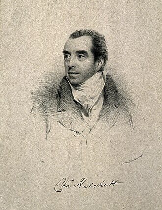
columbium; tantalum; their false identity
1801-1809
III. An analysis 1802, Ekeberg 1802, XV. On the 1809
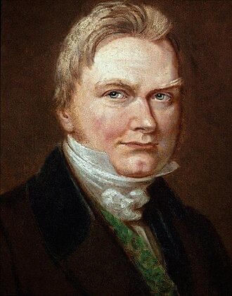
lithium
1817-1818
Arfwedson 1818, Berzelius 1818
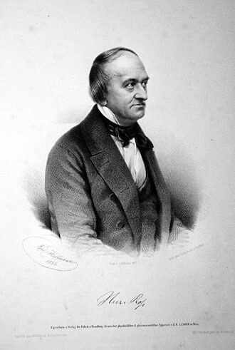
niobium, pelopium; untangling Nb and Ta
1844-1866
Rose 1844, Rose 1846, Marignac 1866
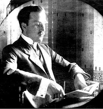
crystal pulling
1916-1917
Czochralski 1918
structure survey listing LiNbO3
1928
Zachariasen 1928
ferroelectricity
1949
Matthias & Remeika 1949
phase diagram
1958
Reisman & Holtzberg 1958
the crystal's characterization and first devices
1964-1985
Curie temperature; Czochralski growth; monographs
1965-1999
Smolenskii et al. 1966, Fedulov & al. 1965
hologram fixing, doped LN
1971-1972
Amodei & Staebler 1971b, Amodei et al. 1972
band-transport equations
1977-1979
Kukhtarev et al. 1978a
bulk photovoltaic theory
1977-1992
Fridkin 1977, Belinicher & Sturman 1980
Zn, In dopants; monograph
1990-2009
Volk et al. 1990, Volk & Wöhlecke 2009
IDT
1965
White & Voltmer 1965
SAW cuts
1972-1976
Yamanouchi & Shibayama 1972, Shibayama et al. 1976
periodic domains; optical superlattices
1980-1997
Feng et al. 1980, Zhu et al. 1997
MgO:LN
1980-1983
Eleventh International Quantum 1980, Ji-guo et al. 1983
MgO:LN journal report
1984
Bryan et al. 1984
QPM theory, PPLN, OPOs
1987-1997
Fejer et al. 1992, Myers et al. 1995a
electric-field poling
1993
Yamada et al. 1993
stoichiometric growth
1992-2001
Kitamura et al. 1992, Oxide Corporation 2026
direct-bonded PPLN; squeezers
2003-2021
Nishida et al. 2003, Kashiwazaki et al. 2021
drift-assured Ti:LN; coherent LN; TFLN
1992-2021
Seino et al. 1992, Fujitsu 2009, Fujitsu 2021
LN modulators
1993-
Nagata & Kiuchi 1993, Sumitomo Osaka Cement 2026
crystals from 1967; first commercial modulator 1985
1967-2011
Becker 1988, Gooch & Housego 2026
Ti:LN modulator industry
1995-2003
Er:LN lasers; LNOI wires
1990-2012
Brinkmann et al. 1991, Hu et al. 2009
layer transfer
1995-2010
Bruel 1995, Pijolat et al. 2008
crystal ion slicing
1998
Levy et al. 1998
bonded LNOI, microrings
2004-2012
Rabiei & Gunter 2004, Poberaj et al. 2012
LNOI wafer supply
2010-
NANOLN 2026
TFLN revival; startup
2014-2026
Zhang et al. 2017, Wang et al. 2018b
hybrid Si/LN; DP-IQ
2019-2022
He et al. 2019, Xu et al. 2022, Wang et al. 2022
LN lasers; TFLT
2023-2024
Snigirev et al. 2023, Wang et al. 2024
| Image | Author | License | File page |
|---|---|---|---|
| Heinrich Rose, lithograph (Austrian National Library original) | Rudolph Hoffmann (lithograph) | Public domain | Wikimedia Commons |
| Jons Jacob Berzelius, portrait, 1826 | John Way (per file page) | Public domain | Wikimedia Commons |
| Charles Hatchett, lithograph by W. Drummond, 1836 | Wellcome Collection | CC BY 2.0 | Wikimedia Commons |
| Jan Czochralski, about 1910 | Unknown | Public domain | Wikimedia Commons |
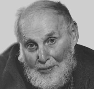
| Arthur Ashkin at Nobel week, 2018-12-08 | Bengt Nyman | CC BY 2.0 | Wikimedia Commons |
| Bell Telephone Laboratories, Murray Hill NJ, 1942 (Library of Congress, Gottscho-Schleisner) | Gottscho-Schleisner Collection | Public domain | Wikimedia Commons |
| Small LN crystal in a NIST quantum-optics setup, 2012 | National Institute of Standards and Technology | Public domain (NIST, US Government work) | Wikimedia Commons |
| LN single-crystal wafer | Smithy71 | CC0 | Wikimedia Commons |
Licenses checked on Wikimedia Commons 2026-10-25; resized copies. Rows without a portrait have no image cleared as public domain, CC0 or CC BY.


